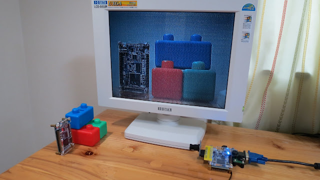
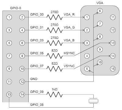
Friday, December 6, 2013Demo System Revised (Camera Control)Though a little belated, I’ve uploaded a renewed demo system. The link to download the demo is the same (relm_demo.jar) as it was. The new demo includes almost all the contents the previous demo had, however, these two versions has no software compatibility due to the changes in the new circuit. The most crucial addition is a CMOS sensor camera control, while capability of SVGA resolution (800 x 600) and a warm reset function are also added. The change in the JTAG communication specs has achieved a little bit faster image transfer. The demo system includes the programs listed below. reset.rb vga.rb svga.rb gsensor.rb led.rb camera.rb
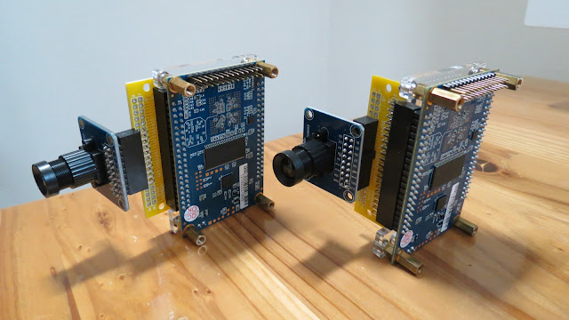
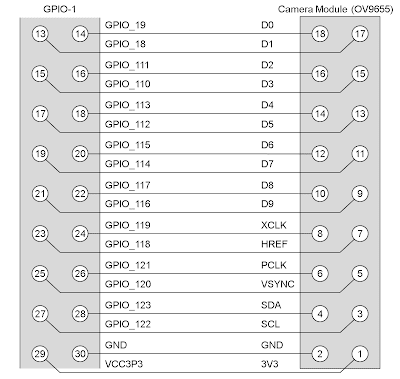
External CMOS sensor uses aitendo’s camera module (OV9655). Also with aitendo’s conversion PCB, as the FPGA pins are assigned in tune with this camera module, it requires no more burdensome wiring than attaching two pin sockets.
This demo is an example of displaying inputs from camera directly on the screen. However, in case of applying this camera in robot control, the system bears the functions of image recognition and motor control instead of VGA output. Just by mounting a simple face detection algorithm as image recognition, it easily realizes a robot to come towards a person’s face. |
Monday, August 12, 2013Demo System RevealedHere, I am introducing a tangible demo of register-less multiprocessor system. This demo system is a register-less multiprocessor with 16 cores installed on a commercial FPGA board DE0-Nano enabling the download and execution of programs by host PC. The main contents of this demonstration are VGA ouput with on-board SDRAM as framebuffer and scrolling the viewing area by accelerometer. Thanks to no disarray in instruction execution timing due to accessing cache memory, register-less multiprocessor system benefits users with capability of device control with rigorous timing directly via software. Here, making the best of this capability, the demo system leaves almost all complicated control on SDRAM to software applications. To run the demo system, it requires just downloading and executing a Jar file (relm_demo.jar) on host PC connected to DE0-Nano board. However, Java Runtime Environment (JRE) and USB-Blaster driver need to be installed beforehand. There would be no problem in an environment where demo programs supplied with DE0-Nano work well. Hopefully the idea was to offer a demonstration viable with DE0-Nano board alone.
In the above picture, a piezoelectric sounder is installed in the empty area of the board but is not used in this demonstration. You can leave this sounder out, if you don’t need sound or worry about piezoelectric element destroying the FPGA board. Execution of “relm_demo.jar” invokes downloading a JRuby Jar file through the internet when JRuby execution environment is not loaded yet. The downloaded “jruby-complete.jar” is stored in the same folder of “relm_demo.jar” and eliminates the need for downloading it again.
Upon the completion of downloading JRuby execution environment, the demo system starts running.
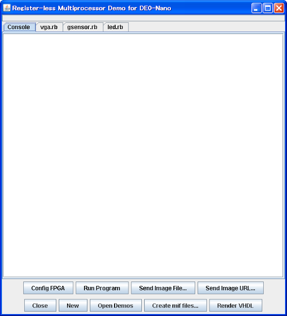
Connect host PC to DE0-Nano and then click “Config FPGA” to execute the configuration of the multiprocessor circuit. Right after configuration, a program loader is executed as one of 16 threads, while all the other threads are halted. The program loader rewrites main memory and SDRAM along with data sent via JTAG from host PC. This way enables rewriting and launching software applications without reconfiguration. Then execute the demo program once configuration is completed. Firstly, let’s try a demonstration viable with DE0-Nano board alone. Select the tab of “led.rb” and click “Run Program” to start once a Ruby program appears in the editor, and then LED on DE0-Nano board starts flashing. As you see here, the demo program is described as Ruby codes, and so is forwarded to and executed on FPGA in the demo environment. However, because this demo system makes up only a assembly-language-like domain-specific language based on Ruby, users are to create software applications by relatively low-level program description. Unfortunately, it doesn’t enable executing common Ruby codes on FPGA. Then next, let’s go on to a higher-level demonstration with the attached VGA output circuit. Click “Config FPGA,” then select the tab of “vga.rb” after finishing configuration and do “Run Program” to start. Connect the output of the VGA circuit to a display you have, and you are supposed to see random patterns of SDRAM initial state on the screen. In the photo below, the left display is for host PC and the right one is for VGA output of FPGA board. In this condition, click “Send Image URL…” to input the URL of an image of Mt.Fuji used in a Wikipedia article (http://upload.wikimedia.org/wikipedia/ja/3/3e/MtFuji_FujiCity.jpg) as an example — you can copy and paste the string of URL by Ctrl+V. Though forwarding data takes a while, you will see the image of Mt.Fuji on the screen for VGA output. With the image active on the screen, select “gsensor.rb” and click “Run Program,” and you can scroll the whole image along with the tilt of DE0-Nano board. In this condition, it is also possible to forward another image to the right screen —— and you can still scroll the viewing area by moving DE0-Nano board during image transfer. This proves that threads of scrolling image by accelerometer and writing image data to SDRAM by program loader are executed separately in parallel. In fact, 4 threads listed below are active at this time.
In addition, the LED flashing demo, if you start it, will run smoothly with no problem. Though it is possible to execute simultaneously up to 16 threads as many as the number of processor cores, the demo system has no function yet to halt each individual thread from host PC. However, the sure way to get back to the initial state with program loader alone is to execute “Config FPGA.” You can run your own program by altering or changing programs via the editor. For example, alter the parameter value of “_wait 1000000” in “led.rb” and click “Run Program,” so that you can change LED flashing speed. Click “New” and pop up a “*Scratch*” tab, so that you can create a new program from the beginning. However, because the demo system has no function to save these alterations, it would be better to import the demo Jar file via Eclipse if you’d like to try this demo system in your program development. When you click “Create mif files…,” you are to have related files (jtag.rb, asm.rb, de0nano.rb, mif.rb) open for reference and then a question dialog “Create mif files?” appears. If you answer “Yes” to the question, memory initialization data files necessary for logic synthesis are created. This memory initialization data include binary code of the program loader. While I am planning to upload instruction of descriptions for software applications later on, it might be possible to understand it by reviewing Ruby codes in asm.rb and de0nano.rb. “Render VHDL” has no direct function in program execution but enables outputting VHDL code for logic synthesis. Actually, the VHDL code is automatically created by Ruby programs, and the codes of these Ruby programs are also displayed at tabbed document interface for reference. It is theoretically possible for users to get to know all technical contents by perusing these programs as well. Just to tell you, the output VHDL code include a “spell” in the first line to pretend as a Ruby code to deal with accidental execution by “Run Program.” While all technological details including Java source codes are in the Jar file, it would be still very difficult for users to advance their own program development alone without explanation. I am going to carry on further explanation based on this tool from now on. |
Thursday, May 23, 2013Instruction SetThe processor about to be on this web accesses its internal memory by 36-bit width consisting of 4-bit opcode and 32-bit data. At fetching an instruction, the 32-bit data is retrieved along with the 4-bit opcode and defined as operand Y at instruction execution.
opcode (4-bit) operand Y (32-bit)
The registers consist of program counter PC and 33-bit long accumulator Acc which includes 32-bit register X and 1-bit carry flag C.
program counter PC
Accumlator Acc (33-bit): carry flag C register X (32-bit)
FPGA (EP4CE22) on DE0-Nano board can provide 36bits x 16k words internal memory, enabling 14-bit program counter PC. Among other instructions, locking flag (lock) for mutual exclusion keeps the internal state unique to each processor element. The locking flag is set on by LOCK (or TRYLOCK) instruction and reset by UNLOCK instruction. Setting the locking flag can be done only at the executing processor, while resetting is executable at any processor by specifying target processors with operand. The below-attached table shows instruction codes and their functions as the changes in internal state. Please be aware that the contents are temporary and may be changed along with adjustments in actual implementation.
Basically, the functions of instructions are determined by 4-bit opcode, while some instructions like conditional jumps use the upper 4 bits of operand Y for expanding instruction. JUMP instruction is to change the value of PC according to conditions and after that, until the lower bits of PC accords to the value of memory bank, to execute HALT instruction internally in order to wait for rotation. Writing back to memory by PUT instruction is actually delayed until the thread reaches the target memory bank. In this case, if another writing instruction to a bank is issued when prior writing to this bank is not completed (collision=1), the instruction is once retried as PC := PC until all the delayed writing is completed in the waiting time of one cycle rotation and then executed again. In this second execution, the writing instruction is surely completed as all other writing tasks are already done. On rewriting operand by PUT instruction, the related opcode is also rewritten with the value of the upper 4 bits of Y. This method is for such reasons as better efficiency of having opcode and operand in the same memory by using parity bits and more convenience of atomic rewriting particularly for exclusive operation. On the other hand, it is also a bother in hand-coding to have to specify opcode even when only operand needs to be rewritten. The instruction set released here is basically designed on the assumption that these tasks are to be automated by compiler or other tools. The biggest thorn in designing here is random-access readout. The processor employs DATA instruction as the minimum required to enable such functions as array and table. DATA instruction assigns the value of operand Y to register X, just like LOAD instruction does, and simultaneously executes a jump to the address which is specified by register X prior to execution of the value assignment. The basic way of use is to assign a return address to register X and execute a jump to a target DATA instruction, which achieves random access by changing destination address of the jump. Though, it is totally inefficient to rewrite operand of every jump instruction. Curiously enough, however, just using a same instruction can solve this thorny problem. For example, here we place a DATA instruction with operand value 123 as data at the address 1000. By the code from the address 100, assign 1000 to register X by LOAD 1000, and then, at the next address 101, execute a DATA instruction with operand 102, the next instruction address. And then, as the result of executing the DATA instruction at the address 101, the value of register X becomes 102, and jump to the address 1000. Subsequently, the DATA instruction at the address 1000 is executed and then the value of register X becomes 123, which triggers jumping to the address 102. As the result, it looks as if the DATA instruction at the address 101 has got data at the address pointed by register X (X := [X]) and additionally worked as an instruction to jump to the address specified by operand (PC := Y). Because these DATA instructions at the addresses 101 and 1000 execute the same action but have completely different meanings in the whole program, I’d like to assign a different name GET to the same opcode at the address 101.
Random-access readout is very low-cost in terms of hardware because it only requires mounting a simple instruction. On the other hand, it becomes costly at the point of execution due to waiting time for rotation, as it needs to have jump operation executed twice. Particularly in the above-mentioned case, which has assigned the next address of the instruction to the return address of GET instruction, it inevitably costs waiting time for one cycle rotation. If it is possible to place GET instruction, DATA instruction and return address in adjoining memory banks, it reduces waiting time for rotation as short as just for two instructions period. Though it isn’t that simple in practice because there would be some GET instructions sharing access to the same DATA instruction, still well-designed arrangement of instructions and data could improve efficiency in instruction execution. This kind of optimization technology could develop as a very interesting subject for study from now on. | ||||||||||||||||||||||||||||||||||||||||||||||||||||||||||||||||||||||||||||||||||||||||||||||||||||||||||||||||||||||||||||||||||||||||||||||||||||||||||||||||||||||||||||||||
Wednesday, May 22, 2013To Introduce JRubyIn parallel with processor designing for DE0-Nano, I am developing environments related to JRuby. JRuby is a Ruby environment workable on a Java virtual machine and can be so easily implemented just through a Jar file. The language Ruby has a high degree of flexibility and enables structuring another language (domain-specific language) on itself. Designing processor circuits requires the use of such hardware description languages as VHDL and Verilog HDL for logic synthesis. But it’s a hard work to write down a large-scale circuit for multiprocessor directly without CAD. Therefore, here I employ a method of automatically generating a VHDL code based on higher-level descriptions written by Ruby. I am also planning to build compilers based on Ruby. Having a call facility to DLL in the Windows environment, JRuby enables access to JTAG itself instead of JNA. And so, here I am offering a JTAG demo program (jtag_demo.jar) based on JRuby. As the Jar file of JRuby (jruby-complete.jar) is pretty large, the demo program does not include it but is to invoke automatic downloading the latest version through the internet.
Put the downloaded file (jruby-complete.jar) in the same folder of the demo program (jtag_demo.jar) or the Java extensions folder (jre/lib/ext), and next time on it will be workable without downloading. This way facilitates distributing circuit data and configuration programs in a very compact file alone. You can refer to the Java and Ruby source codes (to be precise, executable scripts of Ruby) included in the Jar file to use a similar mechanism. |
Wednesday, March 27, 2013JTAG Configuration by JavaTo drive the nail home, now let’s try configuration (rewriting the circuit) of FPGA by JTAG. Firstly, please have a try to download the Jar file (jtag_demo.jar) and execute while keeping DE0-Nano in connection with USB cable. This is supposed to be compatible to 64-bit environment, which is not tested yet though.
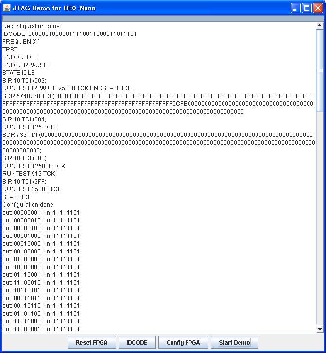
The above image shows the result of executing 4 commands of “Reset FPGA,” “IDCODE,” “Config FPGA” and “Start Demo” one after another, for example. “Reset FPGA” is a command to forcefully configure FPGA, and, in case of DE0-Nano, loads the circuit in the EPCS64 on the board. “IDCODE” is a command to read 32-bit IDCODE of the device “EP4CE22.” “Config FPGA” is to execute a SVF file and configure FPGA. The SVF player has only crucial minimal capabilities, while many other functions such as checking TDO are left out. The last “Start Demo” enables observing I/O data via JTAG communication demonstration (except changing speed and halting by pushing buttons) which appeared in the previous article. To tell you the truth, this command can work with no error even before configuration, but then the output data cast no impact on LED. As this operation requires complicated processing such as execution of SVF and GUI, it would be all the less readable to combine all processes into single Java code. Therefore, I split it into three parts, JTAG library and basic GUI (JTAG.java) as a relatively generic part, execution of SVF (SVFPlayer.java) and demo application (JTAG_Demo.java). With a split library, the demo application part has a very simple design. A button appears in display upon the creation of a JTAG.GUI class instance. While having to describe what you’d like to run in onClick() method, you have little need to write down raw data by write() method thanks to additional methods: state() method to transit JTAG state for SVF execution and shift() method for SHIFT_DR/SHIFT_IR. SVFPlayer class is a derived class of JTAG.GUI, which requires appointing button name and resource name of SVF as generation parameters.
import info.relm.JTAG;
import info.relm.SVFPlayer;
public class JTAG_Demo extends JTAG {
    public static void main(String[] args) {
        GUI.title("JTAG Demo for DE0-Nano");
        new GUI("Reset FPGA") {
            public void onClick() {
                reset();
                state("RESET", "IRSHIFT");
                shift(10, 0x1);
                state("IREXIT1", "IRUPDATE");
                text.append("Reconfiguration done.n");
            }
        };
        new GUI("IDCODE") {
            public void onClick() {
                reset();
                state("RESET", "IRSHIFT");
                shift(10, 0x6);
                state("IREXIT1", "DRSHIFT");
                readBytes(4, 0);
                text.append("IDCODE: " +
                    Long.toBinaryString(0xffffffff00000000L |
                    read(4)[0]).substring(32) + 'n');
            }
        };
        new SVFPlayer("Config FPGA", "jtag_led.svf");
        new GUI("Start Demo", "Stop Demo") {
            public void onClick() {
                reset();
                state("RESET", "IRSHIFT");
                shift(10, 0xe);
                state("IREXIT1", "DRSHIFT");
                shift(9, 0x100);
                state("DREXIT1", "DRSHIFT");
                flush();
                try {
                    for (int lfsr = 1; ; Thread.sleep(10)) {
                        readBytes(1, lfsr);
                        shift(1, 1);
                        state("DREXIT1", "DRSHIFT");
                        text.append("out: " +
                            Integer.toBinaryString(lfsr | 256).substring(1) +
                            "tin: " +
                            Integer.toBinaryString(read(1)[0] | 256).substring(1) +
                            'n');
                        if (((lfsr <<= 1) & 256) != 0) lfsr ^= 0x171;
                    }
                } catch (InterruptedException e) {}
                shift(9, 0x100);
                state("DREXIT1", "DRUPDATE");
            }
        };
    }
}
It enables FPGA configuration without setting up Quartus II. |
