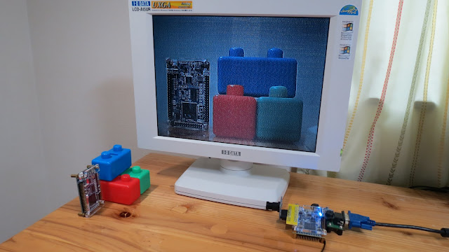
Friday, December 6, 2013Demo System Revised (Camera Control)Though a little belated, I’ve uploaded a renewed demo system. The link to download the demo is the same (relm_demo.jar) as it was. The new demo includes almost all the contents the previous demo had, however, these two versions has no software compatibility due to the changes in the new circuit. The most crucial addition is a CMOS sensor camera control, while capability of SVGA resolution (800 x 600) and a warm reset function are also added. The change in the JTAG communication specs has achieved a little bit faster image transfer. The demo system includes the programs listed below. reset.rb vga.rb svga.rb gsensor.rb led.rb camera.rb
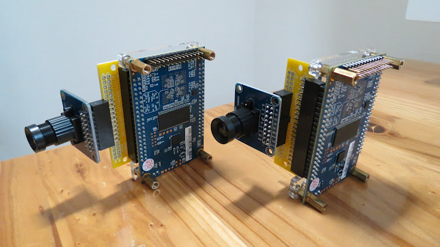
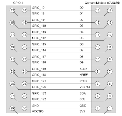
External CMOS sensor uses aitendo’s camera module (OV9655). Also with aitendo’s conversion PCB, as the FPGA pins are assigned in tune with this camera module, it requires no more burdensome wiring than attaching two pin sockets.
This demo is an example of displaying inputs from camera directly on the screen. However, in case of applying this camera in robot control, the system bears the functions of image recognition and motor control instead of VGA output. Just by mounting a simple face detection algorithm as image recognition, it easily realizes a robot to come towards a person’s face. |
Monday, August 12, 2013Demo System RevealedHere, I am introducing a tangible demo of register-less multiprocessor system. This demo system is a register-less multiprocessor with 16 cores installed on a commercial FPGA board DE0-Nano enabling the download and execution of programs by host PC. The main contents of this demonstration are VGA ouput with on-board SDRAM as framebuffer and scrolling the viewing area by accelerometer. Thanks to no disarray in instruction execution timing due to accessing cache memory, register-less multiprocessor system benefits users with capability of device control with rigorous timing directly via software. Here, making the best of this capability, the demo system leaves almost all complicated control on SDRAM to software applications. To run the demo system, it requires just downloading and executing a Jar file (relm_demo.jar) on host PC connected to DE0-Nano board. However, Java Runtime Environment (JRE) and USB-Blaster driver need to be installed beforehand. There would be no problem in an environment where demo programs supplied with DE0-Nano work well. Hopefully the idea was to offer a demonstration viable with DE0-Nano board alone.
In the above picture, a piezoelectric sounder is installed in the empty area of the board but is not used in this demonstration. You can leave this sounder out, if you don’t need sound or worry about piezoelectric element destroying the FPGA board. Execution of “relm_demo.jar” invokes downloading a JRuby Jar file through the internet when JRuby execution environment is not loaded yet. The downloaded “jruby-complete.jar” is stored in the same folder of “relm_demo.jar” and eliminates the need for downloading it again.
Upon the completion of downloading JRuby execution environment, the demo system starts running.
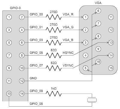
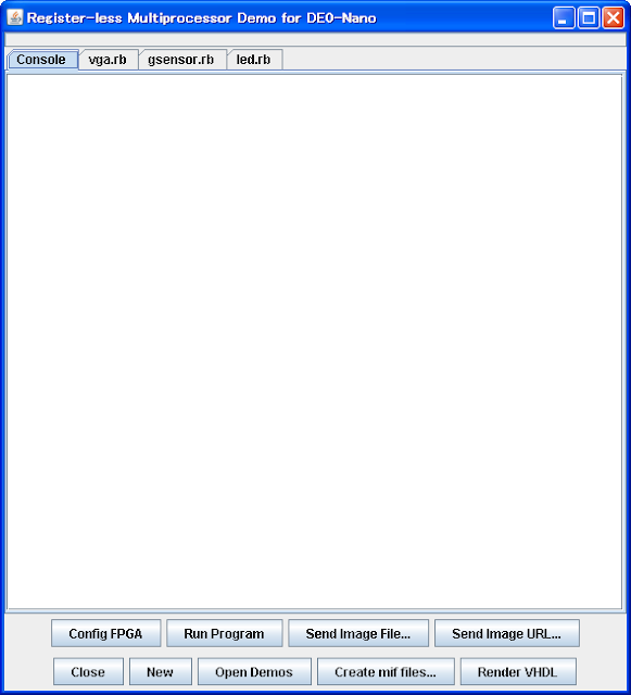
Connect host PC to DE0-Nano and then click “Config FPGA” to execute the configuration of the multiprocessor circuit. Right after configuration, a program loader is executed as one of 16 threads, while all the other threads are halted. The program loader rewrites main memory and SDRAM along with data sent via JTAG from host PC. This way enables rewriting and launching software applications without reconfiguration. Then execute the demo program once configuration is completed. Firstly, let’s try a demonstration viable with DE0-Nano board alone. Select the tab of “led.rb” and click “Run Program” to start once a Ruby program appears in the editor, and then LED on DE0-Nano board starts flashing. As you see here, the demo program is described as Ruby codes, and so is forwarded to and executed on FPGA in the demo environment. However, because this demo system makes up only a assembly-language-like domain-specific language based on Ruby, users are to create software applications by relatively low-level program description. Unfortunately, it doesn’t enable executing common Ruby codes on FPGA. Then next, let’s go on to a higher-level demonstration with the attached VGA output circuit. Click “Config FPGA,” then select the tab of “vga.rb” after finishing configuration and do “Run Program” to start. Connect the output of the VGA circuit to a display you have, and you are supposed to see random patterns of SDRAM initial state on the screen. In the photo below, the left display is for host PC and the right one is for VGA output of FPGA board. In this condition, click “Send Image URL…” to input the URL of an image of Mt.Fuji used in a Wikipedia article (http://upload.wikimedia.org/wikipedia/ja/3/3e/MtFuji_FujiCity.jpg) as an example — you can copy and paste the string of URL by Ctrl+V. Though forwarding data takes a while, you will see the image of Mt.Fuji on the screen for VGA output. With the image active on the screen, select “gsensor.rb” and click “Run Program,” and you can scroll the whole image along with the tilt of DE0-Nano board. In this condition, it is also possible to forward another image to the right screen —— and you can still scroll the viewing area by moving DE0-Nano board during image transfer. This proves that threads of scrolling image by accelerometer and writing image data to SDRAM by program loader are executed separately in parallel. In fact, 4 threads listed below are active at this time.
In addition, the LED flashing demo, if you start it, will run smoothly with no problem. Though it is possible to execute simultaneously up to 16 threads as many as the number of processor cores, the demo system has no function yet to halt each individual thread from host PC. However, the sure way to get back to the initial state with program loader alone is to execute “Config FPGA.” You can run your own program by altering or changing programs via the editor. For example, alter the parameter value of “_wait 1000000” in “led.rb” and click “Run Program,” so that you can change LED flashing speed. Click “New” and pop up a “*Scratch*” tab, so that you can create a new program from the beginning. However, because the demo system has no function to save these alterations, it would be better to import the demo Jar file via Eclipse if you’d like to try this demo system in your program development. When you click “Create mif files…,” you are to have related files (jtag.rb, asm.rb, de0nano.rb, mif.rb) open for reference and then a question dialog “Create mif files?” appears. If you answer “Yes” to the question, memory initialization data files necessary for logic synthesis are created. This memory initialization data include binary code of the program loader. While I am planning to upload instruction of descriptions for software applications later on, it might be possible to understand it by reviewing Ruby codes in asm.rb and de0nano.rb. “Render VHDL” has no direct function in program execution but enables outputting VHDL code for logic synthesis. Actually, the VHDL code is automatically created by Ruby programs, and the codes of these Ruby programs are also displayed at tabbed document interface for reference. It is theoretically possible for users to get to know all technical contents by perusing these programs as well. Just to tell you, the output VHDL code include a “spell” in the first line to pretend as a Ruby code to deal with accidental execution by “Run Program.” While all technological details including Java source codes are in the Jar file, it would be still very difficult for users to advance their own program development alone without explanation. I am going to carry on further explanation based on this tool from now on. |
