Thursday, May 23, 2013Instruction SetThe processor about to be on this web accesses its internal memory by 36-bit width consisting of 4-bit opcode and 32-bit data. At fetching an instruction, the 32-bit data is retrieved along with the 4-bit opcode and defined as operand Y at instruction execution.
opcode (4-bit) operand Y (32-bit)
The registers consist of program counter PC and 33-bit long accumulator Acc which includes 32-bit register X and 1-bit carry flag C.
program counter PC
Accumlator Acc (33-bit): carry flag C register X (32-bit)
FPGA (EP4CE22) on DE0-Nano board can provide 36bits x 16k words internal memory, enabling 14-bit program counter PC. Among other instructions, locking flag (lock) for mutual exclusion keeps the internal state unique to each processor element. The locking flag is set on by LOCK (or TRYLOCK) instruction and reset by UNLOCK instruction. Setting the locking flag can be done only at the executing processor, while resetting is executable at any processor by specifying target processors with operand. The below-attached table shows instruction codes and their functions as the changes in internal state. Please be aware that the contents are temporary and may be changed along with adjustments in actual implementation.
Basically, the functions of instructions are determined by 4-bit opcode, while some instructions like conditional jumps use the upper 4 bits of operand Y for expanding instruction. JUMP instruction is to change the value of PC according to conditions and after that, until the lower bits of PC accords to the value of memory bank, to execute HALT instruction internally in order to wait for rotation. Writing back to memory by PUT instruction is actually delayed until the thread reaches the target memory bank. In this case, if another writing instruction to a bank is issued when prior writing to this bank is not completed (collision=1), the instruction is once retried as PC := PC until all the delayed writing is completed in the waiting time of one cycle rotation and then executed again. In this second execution, the writing instruction is surely completed as all other writing tasks are already done. On rewriting operand by PUT instruction, the related opcode is also rewritten with the value of the upper 4 bits of Y. This method is for such reasons as better efficiency of having opcode and operand in the same memory by using parity bits and more convenience of atomic rewriting particularly for exclusive operation. On the other hand, it is also a bother in hand-coding to have to specify opcode even when only operand needs to be rewritten. The instruction set released here is basically designed on the assumption that these tasks are to be automated by compiler or other tools. The biggest thorn in designing here is random-access readout. The processor employs DATA instruction as the minimum required to enable such functions as array and table. DATA instruction assigns the value of operand Y to register X, just like LOAD instruction does, and simultaneously executes a jump to the address which is specified by register X prior to execution of the value assignment. The basic way of use is to assign a return address to register X and execute a jump to a target DATA instruction, which achieves random access by changing destination address of the jump. Though, it is totally inefficient to rewrite operand of every jump instruction. Curiously enough, however, just using a same instruction can solve this thorny problem. For example, here we place a DATA instruction with operand value 123 as data at the address 1000. By the code from the address 100, assign 1000 to register X by LOAD 1000, and then, at the next address 101, execute a DATA instruction with operand 102, the next instruction address. And then, as the result of executing the DATA instruction at the address 101, the value of register X becomes 102, and jump to the address 1000. Subsequently, the DATA instruction at the address 1000 is executed and then the value of register X becomes 123, which triggers jumping to the address 102. As the result, it looks as if the DATA instruction at the address 101 has got data at the address pointed by register X (X := [X]) and additionally worked as an instruction to jump to the address specified by operand (PC := Y). Because these DATA instructions at the addresses 101 and 1000 execute the same action but have completely different meanings in the whole program, I’d like to assign a different name GET to the same opcode at the address 101.
Random-access readout is very low-cost in terms of hardware because it only requires mounting a simple instruction. On the other hand, it becomes costly at the point of execution due to waiting time for rotation, as it needs to have jump operation executed twice. Particularly in the above-mentioned case, which has assigned the next address of the instruction to the return address of GET instruction, it inevitably costs waiting time for one cycle rotation. If it is possible to place GET instruction, DATA instruction and return address in adjoining memory banks, it reduces waiting time for rotation as short as just for two instructions period. Though it isn’t that simple in practice because there would be some GET instructions sharing access to the same DATA instruction, still well-designed arrangement of instructions and data could improve efficiency in instruction execution. This kind of optimization technology could develop as a very interesting subject for study from now on. | ||||||||||||||||||||||||||||||||||||||||||||||||||||||||||||||||||||||||||||||||||||||||||||||||||||||||||||||||||||||||||||||||||||||||||||||||||||||||||||||||||||||||||||||||
Tuesday, February 12, 2013Designing MultiprocessorNow, let’s begin with designing a circuit of accumulator machine, the very fundamental element for register-less architecture. Draw a rough block diagram along data flow. Accumulator machines basically flow only program counter (PC) and Accumulator (Acc). Other data such as status flags are left out here.
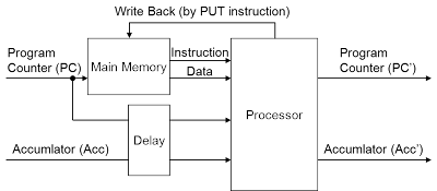
Processor reads instruction and data at a time from main memory based on present internal state (PC, Acc), executes an operation such as arithmetic or jump instruction, and updates internal state to (PC’, Acc’). It also updates main memory at the same time in case of executing a PUT instruction. Connect the new internal state output to the input of present internal state, and just a single processor is done — so easy, isn’t it? To be timed with output of memory access, internal state signals are to be delayed for the same clock number and then input to the processor. As arithmetic instruction and jump instruction can be executed as changes in accumulator and program counter, respectively, the processor basically needs to have only a combinational circuit internally. And CPI (Clocks per Instruction: the number of clock cycle per instruction execution) can be set to 1 on the conditions listed below.
These conditions are not so difficult, as latest embedded memories for FPGA are usually dual ported and enable one-clock access. It is an earnest wish in processor architecture to achieve 1 CPI, and to exceed this, complicated techniques are required such as instruction prefetching and instruction-level parallelism. Therefore, it is better to keep the structure of each processor element as simple as this and to leave performance improvement to multiplying processor cores. Join a number of these processors at inputs and outputs of their internal state in a ring, and a multiprocessor is done. Though main memory is divided into banks and assigned to each processor, this whole structure alone brings a problem of confining processor’s writing by PUT instruction only to its own bank. It could be an idea to use this mechanism in disregard of such inconvenience, but then there is no other tool for data transfer than accumulator, which is not only inconvenient but limits processing performance due to lack of inter-processor communication bandwidth.
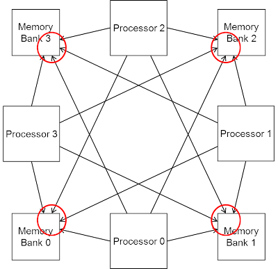
Actually, such a ring-structured (network topology) multiprocessor has an advantage of making circuits simple but has a hardness for random access. The system preferably enables PUT instruction, which executes random access writing, as writing to other banks is an important indirect inter-processor communication. However, a naive way of connecting write signals from every processor to all banks requires each bank to have as many ports as the processors and ruins the simple ring structure.
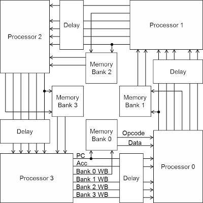
In fact, we can evade the problem of random access writing by loosening memory coherence requirement. For example, even though writing on a hard disk is difficult to achieve promptly due to head seek and rotating time, computers cannot afford to halt until its achievement. Most operating systems clear this problem by queueing data in memory and writing later all at once. Here for our multiprocessor as well, there would be no difference in its actual results even if writing to bank 0 is suspended until next time the bank 0 is read. Therefore, the system here takes the approach of suspending writing data to another bank until a program (or a thread) self reaches the destination bank.
This approach assures a program’s retrieving what it has written in a bank. However, what another program writes in is not promptly reflected in memory contents. Speaking of memory coherence, this approach sustains memory coherence within a program (or a thread) but not for between plural programs (or threads). Nevertheless, all write backs are to be reflected in memory contents within the writing program walk around all the processors. Therefore, implementing programs with consideration to the delay of write backs would cause no problem.
The diagram shows a design with 4 processors, as an example. While this design results in a bit complicated lines along with the increase of write back signals, it guarantees enough bandwidth of data transfer between processors, and moreover, needs every bank only to be dual ported. However, there are much more points to be considered regarding to random access reading. To be continued… |
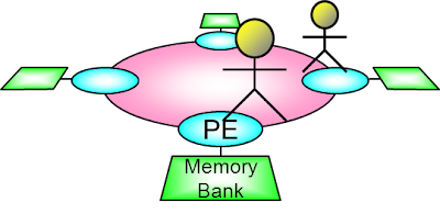
Tuesday, January 22, 2013Accumulator Machine & Self-modificationMultiprocessor system based on register-less architecture can be illustrated in the image below as if tasks run themselves while going round and chasing each other through processor elements.
Inner state information of each task should be as simple and light as possible to move between processors, requiring employment of architecture minimizing register. The most typical of such architecture is accumulator machine. For example, accumulator machine executes such a form of instruction as shown below. ADD memory_address The actual processing this instruction does is to add the value of memory at location memory_address to the value of accumulator Acc, the only general-purpose register of the processor. Acc <= Acc + (memory value at memory_address) While being quite useful for downsizing circuit, accumulator machine is not suitable for speeding up because of increasing memory access. To do “ADD memory_address,” for example, accumulator machine requires at least twice access to memory: once to read the ADD instruction and memory_address and the second time to read the value of memory at the memory_address. Accumulator machine has been almost abandoned as being out of date against current development in processors to minimize memory access. However, except this weak point, accumulator machine has preferable properties to be an element of small-scale multiprocessor. Therefore, I am introducing a technique of equipping small-scale multiprocessor with improved accumulator machine. If processor has register other than accumulator, reading register can replace once of memory access by specifying register number instead of memory address: ADD register_number {Acc <= Acc + (register value)} Even so, reading register value is possible only after having register number fixed and therefore impossible at the same time of reading instruction. Actually, an instruction is executed through at least four stages:
Most of current processors achieve high performance by simultaneously running these stages through pipelining. In reality, however, this technique requires various kinds of efforts to perform well, causing current processors to be complicated. After all, this kind of problem is inevitable, even by using register, unless parameters necessary to run instruction (in case of addition, both left-hand side and right-hand side) are fixed at the same time that the instruction is retrieved. The only solution is to limit instruction parameters to fixed values (immediate/literal). In ADD instruction, it goes like this: ADD immediate {Acc <= Acc + (immediate value)} Processor needs to access memory only once, if it can read instruction and parameters at the same time. Then it goes to addition instantly, and basically has no need for complicated pipeline processing. Of course, programs only with fixed parameters make processor nothing but useless, however, this is solvable by self-modifying code. That is, to be more specific, PUT instruction to replace parameter of instruction at the address indicated by parameter of the PUT instruction with current value of accumulator: PUT instruction_address {[instruction_address] <= Acc} As the parameter of PUT instruction itself is rewritable by another PUT instruction, array and other indirect addressing are also available. PUT instruction makes parameters of every instruction available as general-purpose registers in fact. Self-modification of codes is a rarely-used technique in current processors except special cases. Not only such issues like security and memory protection, but the biggest negative reason seems to be that code’s self-modifying process is quite inefficient in cache memory and instruction pipeline. Register-less architecture spotlights and employs aggressively this out-of-the-mainstream technique of self-modification. That is, register-less architecture is what revives non-mainstream techniques of accumulator machine and self-modifying as elements of small-scale multiprocessor. To be continued… |
Friday, January 18, 2013Multiprocessor & Memory AccessIn recent years, multi-core processors are loaded so commonly in notebook PCs and even mobile devices. And now, even smartphones with quad-core are circulating in the world. Then, why not add more cores? — But it doesn’t go that easily. While there is an argument called Amdahl’s law due to the fact that programs in the world cannot always be parallelized, even if they could be, the lack of memory access throughput inevitably holds down processing performance (Von Neumann bottleneck). In computing, a CPU needs the process of reading a program and data from memory and then writing results to memory. No matter how fast CPU alone operates, it cannot do much as long as it cannot reach memory at the same speed. So, how are current multiprocessors addressing this problem?
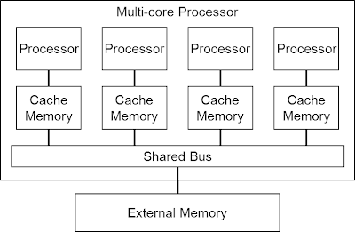
Most multiprocessors in the world are basically configured to have distributed cache memory as shown in the figure above. In this configuration, every processor copies necessary parts of programs and data into cache memory to use, drastically reducing the need for access to shared memory. Usually, cache memory and shared bus run much faster than external shared memory, a multi-core processor enhances its performance along with the increase of its internal processor cores. Since memory access directly determines the performance of processor, cache memory is the component consuming the largest area and most electric power in processor. Cache memory has the original role of covering the difference in the speed of external memory and the inside of processor, but has become indispensable to simultaneous access to memory in multi-core processor due to cache coherency. But in processor with chip-embedded memory, cache memory is of course waste and useless. Then, how can a small-scale multiprocessor with embedded memory be composed? — Firstly, by force.
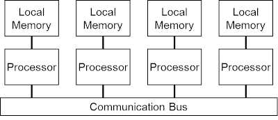
The use of multiport memory theoretically enables direct connection of shared memory and processors. However, it reduces area efficiency (necessary area is said to be proportional to the square of port number) and is unavailable in a FPGA, which usually has up to two ports. Another choice is to assign local memory to each processor and have communication bus, instead of giving up shared memory. This format facilitates designing hardware and so is relatively common — For example, the Cell processor of PS3 has a similar structure.
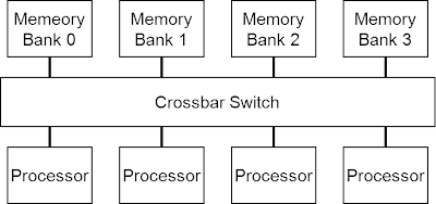
Despite of easy designing hardware, designing software is all the harder. Particularly in small-scale processors, it is out of question to divide already scarce main memory to each processor. The system could be also designed to allow a processor to access local memory of other processors somehow, which, however, seems to be inefficient for its complexity. Another structure is possible by dividing shared memory not per processor but to memory banks corresponding to address areas.
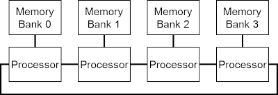
Crossbar switch enables simultaneous access as long as each of processors aims at a different memory bank. But when some processors try to access the same memory bank, all except one are blocked from access to the bank. The problem is that the increasing number of processors rapidly complicates crossbar mechanism. There has been lots of research on how to simplify the mechanism since early times. (Like this study, for example) It brings interesting results if you divide memory into banks by the remainder of each address divided by the number of processors. In the figure attached above, for example, memory banks numbered as 0 through 3 mean the memory areas tagged with the remainders from 0 through 3 of addresses divided by 4. At one point in time, if four processors have execution addresses 100, 201, 302 and 403, respectively, the remainders of these addresses divided by 4 are 0, 1, 2 and 3, thus allowing processors to fetch operation code from respective corresponding memory banks simultaneously. At a next point, execution addresses become 101, 202, 303 and 404, and the remainders are 1, 2, 3 and 0, again enabling simultaneous access to respective memory banks. Likewise, four processors sustain the situation of simultaneous accessibility unless any of them executes a jump instruction. If a group of processors can be shifted in this situation, there would be no need for crossbar mechanism at all. That said, it is impossible to physically rotate processors within an IC, and therefore, the actual method is to transfer entire internal state of every processor by a chain of bus connections.
Since processor’s internal state should naturally include values of all registers, the values as many as the registers a processor has must be sent out to next processor. That means the less registers a processor has, the more efficient implementation could be. This point finds out the feasibility of small-scale multiprocessor based on register-less architecture. To be continued… |
Tuesday, January 15, 2013What is “Register-less Architecture”?“Register-less Architecture” is literally an architecture of a microprocessor omitting register. That said, a processor with no register cannot do anything. Therefore, the processor in this case has minimal register and can also use its main memory as general-purpose register. Several classic processors prior to RISC substituted part of main memory for register. Current high-performance processors, operating by GHz unit internally, depend on lots of register and cache memory. However, the circumstances are different when we use a FPGA as a microcontroller accommodating main memory and a processor. This configuration has no need of external memory, but has to allocate the precious internal memory resource to register file and main memory. Therefore, the more register turns to be the less main memory. As the register and the main memory use the same internal memory after all, there is little effect in reducing access to main memory by using register. In this context, the primary feature of the “register-less architecture” is that the entire memory embedded in a FPGA is available as main memory. Another significant feature of the architecture is multi-core availability. Designing mainboard may sound like mission impossible to hobby users, once multiprocessors emit high-speed signals externally on PCB, but it is achievable just by struggling with EDA tools, as long as it is all about inside FPGA. Once packing multi-core processor and main memory into a FPGA, all you need is a hardware description language for complete design. Therefore, this would be almost the only way for hobby users to design a system with multi-core so far. However, this method requires a multi-core processor with (commonly incredible) compact circuit so as to fit in a FPGA unit. Register-less architecture also serves as a design methodology for it. To be continued… |
