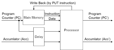
Tuesday, February 12, 2013Designing MultiprocessorNow, let’s begin with designing a circuit of accumulator machine, the very fundamental element for register-less architecture. Draw a rough block diagram along data flow. Accumulator machines basically flow only program counter (PC) and Accumulator (Acc). Other data such as status flags are left out here.
Processor reads instruction and data at a time from main memory based on present internal state (PC, Acc), executes an operation such as arithmetic or jump instruction, and updates internal state to (PC’, Acc’). It also updates main memory at the same time in case of executing a PUT instruction. Connect the new internal state output to the input of present internal state, and just a single processor is done — so easy, isn’t it? To be timed with output of memory access, internal state signals are to be delayed for the same clock number and then input to the processor. As arithmetic instruction and jump instruction can be executed as changes in accumulator and program counter, respectively, the processor basically needs to have only a combinational circuit internally. And CPI (Clocks per Instruction: the number of clock cycle per instruction execution) can be set to 1 on the conditions listed below.
These conditions are not so difficult, as latest embedded memories for FPGA are usually dual ported and enable one-clock access. It is an earnest wish in processor architecture to achieve 1 CPI, and to exceed this, complicated techniques are required such as instruction prefetching and instruction-level parallelism. Therefore, it is better to keep the structure of each processor element as simple as this and to leave performance improvement to multiplying processor cores. Join a number of these processors at inputs and outputs of their internal state in a ring, and a multiprocessor is done. Though main memory is divided into banks and assigned to each processor, this whole structure alone brings a problem of confining processor’s writing by PUT instruction only to its own bank. It could be an idea to use this mechanism in disregard of such inconvenience, but then there is no other tool for data transfer than accumulator, which is not only inconvenient but limits processing performance due to lack of inter-processor communication bandwidth.
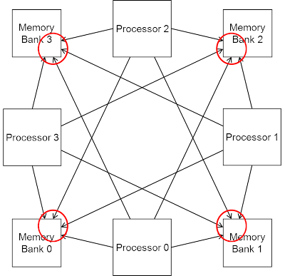
Actually, such a ring-structured (network topology) multiprocessor has an advantage of making circuits simple but has a hardness for random access. The system preferably enables PUT instruction, which executes random access writing, as writing to other banks is an important indirect inter-processor communication. However, a naive way of connecting write signals from every processor to all banks requires each bank to have as many ports as the processors and ruins the simple ring structure.
In fact, we can evade the problem of random access writing by loosening memory coherence requirement. For example, even though writing on a hard disk is difficult to achieve promptly due to head seek and rotating time, computers cannot afford to halt until its achievement. Most operating systems clear this problem by queueing data in memory and writing later all at once. Here for our multiprocessor as well, there would be no difference in its actual results even if writing to bank 0 is suspended until next time the bank 0 is read. Therefore, the system here takes the approach of suspending writing data to another bank until a program (or a thread) self reaches the destination bank.
This approach assures a program’s retrieving what it has written in a bank. However, what another program writes in is not promptly reflected in memory contents. Speaking of memory coherence, this approach sustains memory coherence within a program (or a thread) but not for between plural programs (or threads). Nevertheless, all write backs are to be reflected in memory contents within the writing program walk around all the processors. Therefore, implementing programs with consideration to the delay of write backs would cause no problem.
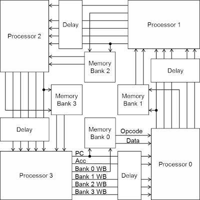
The diagram shows a design with 4 processors, as an example. While this design results in a bit complicated lines along with the increase of write back signals, it guarantees enough bandwidth of data transfer between processors, and moreover, needs every bank only to be dual ported. However, there are much more points to be considered regarding to random access reading. To be continued… |


